Maximus R&D
  • Quick Navigation
  • Home
    • About Pieter Hooijmans
    • About Maximus-R&D
    • Experience >
      • Radar Technology
      • Optical communications
      • Tuners and RF Modules
      • RF IC's
      • Communication Systems
      • Audio and Analogue
      • IC Technology
      • Packaging
    • R&D Processes
    • Services >
      • Client Projects
    • Contact
  • Technology History
    • Piet Hooijmans 1918 - 2006
    • Piet's Home-built Television pt1
    • Piet's Home-built Television pt2
    • EQ40 and EQ80
    • TV Tuner history pt1
    • TV Tuner history pt2
    • TV Tuner history pt3
    • Philips TV remote controls, 1955-1985
    • TV Tuner history pt4
    • TV Tuner history pt5
    • TV Tuner history pt6
    • Digital circuit blocks
    • TRANSDECO
  • Oil Painting

Packaging

Packaging is a very important but broad area. Apart from the odd naked die in some exotic application, 99% of the IC's is sold packaged. This can roughly be divided into three areas:
  1. plastic over-moulded packages (probably 80% of all products)
  2. wafer-level or chip scale packaging (CSP), especially driven by the mobile phone and portable devices markets
  3. modules or hybrid packages, which is essentially everything non-standard.
For the latter category I refer to the page on RF Modules.

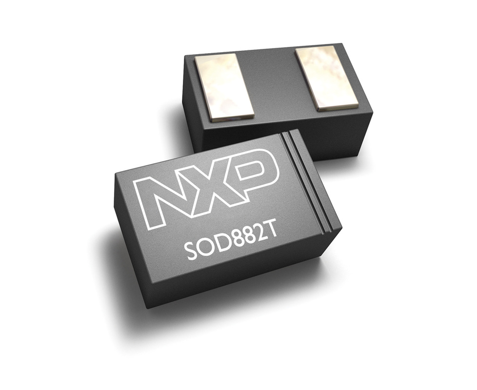
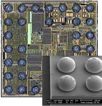
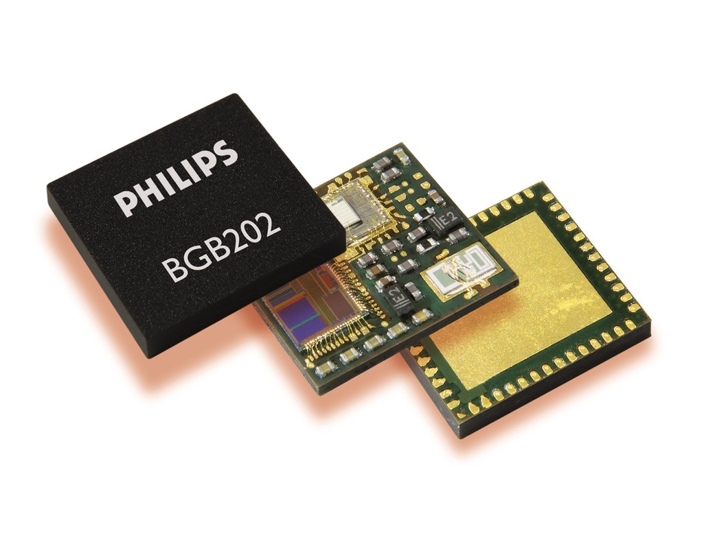
Over the years I have lived through the many diverse and successive families of ever smaller over-moulded IC-packages: from DIL to SSOP to QFN and lead-less. Main drivers: cost and miniaturization. Decisions on these type of platform generations are as complex as CMOS-generation discussions: major investments, long term strategic impact and increasingly make-or-buy or at least 2nd-sourcing discussions.

Next to that there were many different more specialised packages, of which I will only mention a few:
  • vertical packages for discretes
  • power packages, with e.g. clips and soft soldering
  • extremely thin lead-less packages
  • waver level chip scale and bumping, with or without redistribution layers
  • thin packages with internal redistribution lead frames
  • multi-die packages; stacked or adjacent dies
  • BGA's
  • RF packages, including RF Power modules and later plastic over-moulded RF Power
  • Sensor packages with windows for the sensor
  • Au to Cu wire conversion

Foto
Foto
Foto

PCB and substrate technology

Over the years, and especially related to modules or advanced packages, Printed Circuit Boards (PCB) has been a recurring technology.
  • in tuners the PCB was a key element, especially w.r.t. solderability of the wide range of components: from fine pitch SSOP IC's to the all metal tin can
  • RF modules were made on either Al2O3 ceramic substrates or multi-layer FR4 PCB. Major price-performance analysis for each case.
  • Never-ending concept discussions about chip-in-PCB (i.e. naked dies embedded and over-moulded inside a PCB instead of a package). Of course never materialised.

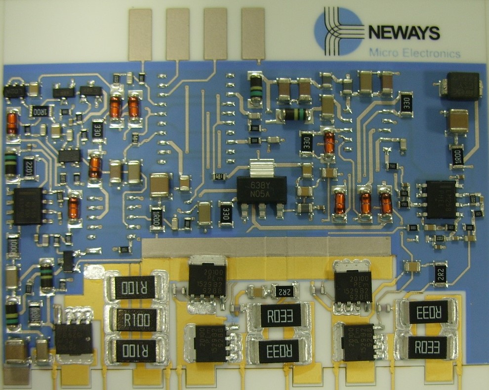
Recently with one of my customers Neways Microelectronics a very interesting project on innovation in the ceramic thick film segment, the primary technology for (automotive) power modules. Even in the oldest technologies innovation is still possible!
BACK
Home
Contact
Picture
Web design by Margot and Pieter Hooijmans using Weebly.
  • Quick Navigation
  • Home
    • About Pieter Hooijmans
    • About Maximus-R&D
    • Experience >
      • Radar Technology
      • Optical communications
      • Tuners and RF Modules
      • RF IC's
      • Communication Systems
      • Audio and Analogue
      • IC Technology
      • Packaging
    • R&D Processes
    • Services >
      • Client Projects
    • Contact
  • Technology History
    • Piet Hooijmans 1918 - 2006
    • Piet's Home-built Television pt1
    • Piet's Home-built Television pt2
    • EQ40 and EQ80
    • TV Tuner history pt1
    • TV Tuner history pt2
    • TV Tuner history pt3
    • Philips TV remote controls, 1955-1985
    • TV Tuner history pt4
    • TV Tuner history pt5
    • TV Tuner history pt6
    • Digital circuit blocks
    • TRANSDECO
  • Oil Painting