Technology definition & development
I am not a process technology expert by profession, so for discussions about HOW to make an IC-technology I have to refer to the physics colleagues. However, over the years I've been heavily involved and responsible for technology analysis and definition. Answering questions like:
Below a summary of the many Si-technologies I've worked with.
- do we need a next generation technology?
- what will be the main drivers for that next Generation? E.g. size or cost reduction, power consumption, performance improvement, feature integration (embedded memories, passives, sensors, ...).
- make or buy (from a foundry)?
- big steps or multiple small steps?
- and of course associated investments (project cost and equipment), resulting wafer cost and the resulting business case for the technology development.
Below a summary of the many Si-technologies I've worked with.
RF Technologies
Dedicated RF performance in combination with silicon integration has always been driven by bipolar technology.
|
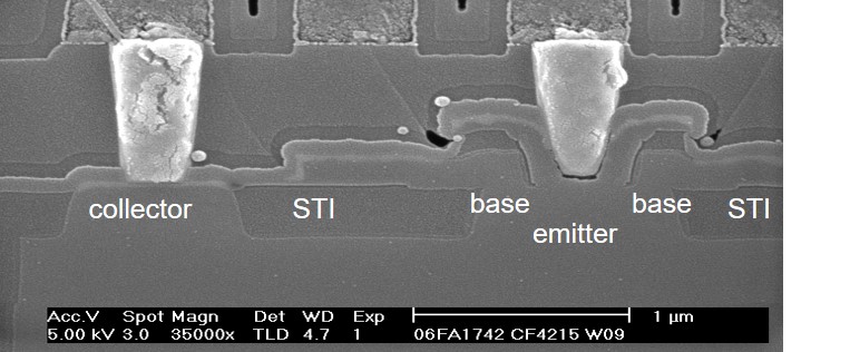
Typical Qubic SiGe bipolar transistor cross section, showing the lateral structure as opposed to the typical vertical MOS build-up.
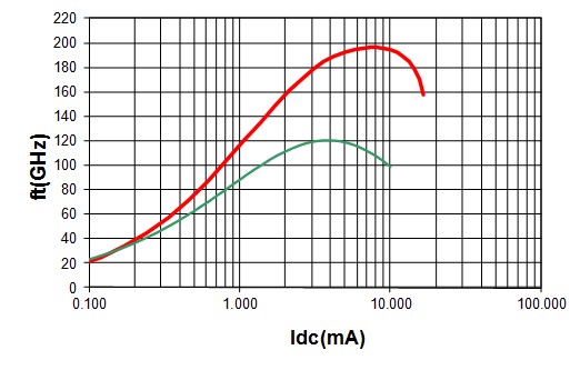
The Qubic4Xi ft-curve in red, showing the effective 200GHz. For comparison in green the curve for 65nm RFCMOS. Although the intrinsic fT of deep sub-micron CMOS is high, the large interconnect parasitics reduce the effective fT to values half those of bipolar.
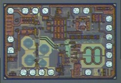
A typical Qubic4X microwave IC, with clearly visible high-quality inductors. This is a satellite down-converter operating at 10-12GHz.
|
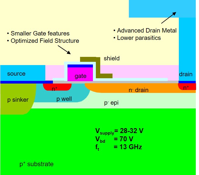
Typical Gen7 silicon LDMOS power transistor cross-section.
|
Of course there are more RF-technologies than BiCMOS. Especially for RF power applications dedicated technologies are required. NXP (now Ampleon) has been one of the two leading players in LDMOS Si-based RF power transistors, as used in all cellular base stations. Over successive generations efficiency and (passive) integration level were driven to increasingly higher levels.
Where LDMOS is no longer efficient (i.e. above a few GHz or at extremely high power densities) III-V technologies come into play. Historically this was GaAs, which we used e.g. for mobile phone RF power amplifiers, the last years a lot of effort went into GaN. On this last one the RF efficiency advantage is undeniable, but the excessive cost structure is a major issue. Time will learn whether GaN will really become as successful as predicted. |
|
RF-CMOS is a quite different technology segment. Here it is not the question how the technology can be optimized (it is simply given as a certain node of baseline CMOS), but how RF-design can still be done given the mediocre technology. Although the intrinsic fT of a CMOS transistor can be very high, the parasitics due to low-ohmic substrates and highly dense interconnect are typically high, reducing the effective performance considerably. The seriously higher design effort, the much higher mask set cost make that RFCMOS solutions are effectively only viable in the specific case of single-chip SoC integration of an RF-transceiver with a much larger digital baseband/controller. Where the resulting medium RF performance must then be accepted as one of the consequences.
RFCMOS yes or no remains one of the most heated debates with respect to technology selection, and will probably remain so for a while. I went through these discussions for the 180, 140, 90, 65 and 40nm nodes, with grey hairs as a result. |
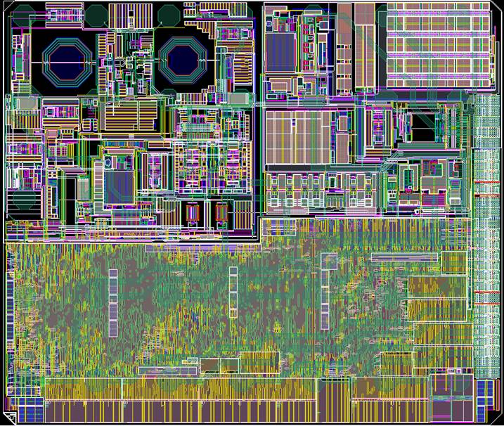
A typical RFCMOS IC, with upper left the RF section, upper right the filter, PLL and power control, and the lower half the purely digital baseband. This one was in 40nm.
|
Power technologies
Like RF, power is a very broad technology area, with many different optimizations for the many power segments. Roughly speaking there are two main segments of power technology:
1. High-voltage/high-power discrete technologies
|
An EZHV 800V die.
A GaN-on-Si 600V power transistor.
|
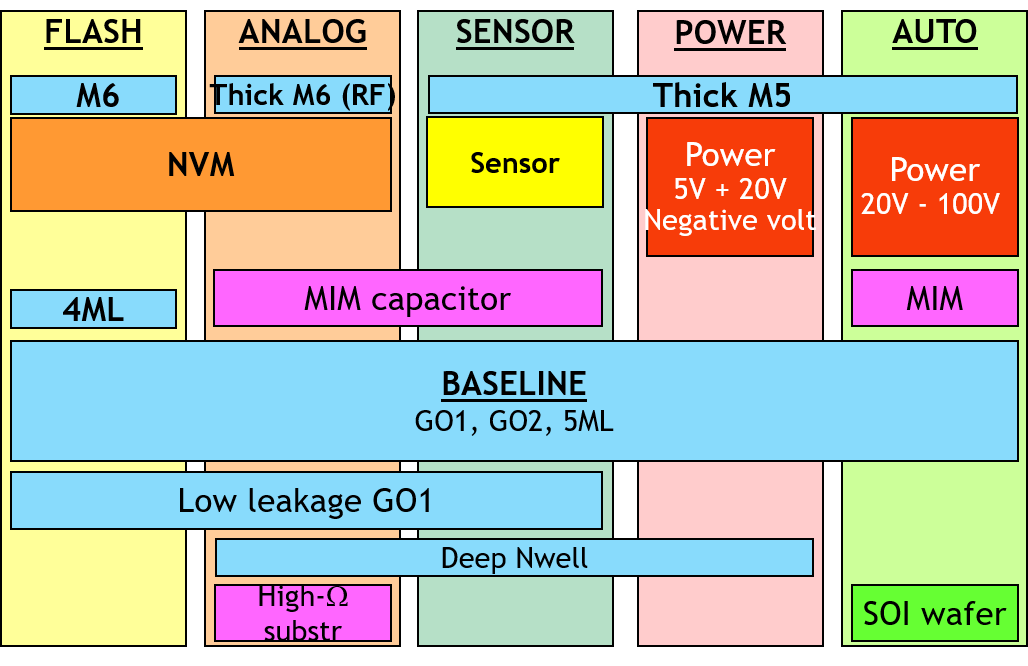
A silicon platform structure within a defined CMOS node, making application-specific optimizations by adding or deleting process modules.
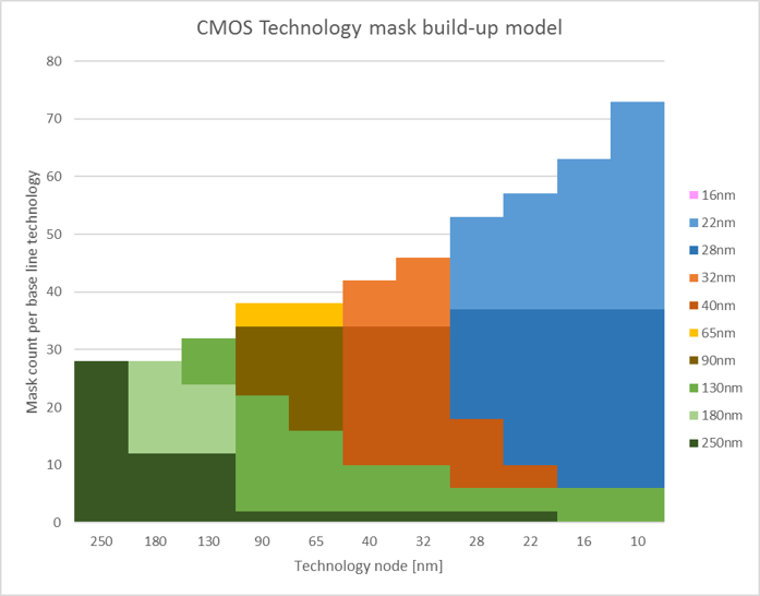
CMOS mask build-up model to simulate wafer and mask cost for each of the CMOS nodes.
|
CMOSIn CMOS there are (for companies like NXP with internal wafer fabs) two types of technology strategy discussions around CMOS:
1. Internal platform extension Although all companies will at one moment stop internal development of the next CMOS node, having the older internal CMOS platforms has a major advantage with respect to cost and supply. Within NXP the last and most cost effective platform was 140nm, ideally suited for the high-performance mixed-signal products we were making. As the main business using this platform I have driven to broaden it as much as possible, adding application-specific features:
2. Foundry CMOS sourcing For baseline CMOS, offered by the foundries (TSMC, Global Foundries, UMC and more) the challenge is to determine (on company level) which nodes are the most efficient to use. This requires structural cost analysis, strategic prediction of what will be become the main nodes (both at market level and within the company) and analysis of the performance and features. Within NXP we went through this process for 110, 90, 65/55, 45/40 and 32/28 nm, within a Maximus consultancy project also down to 16 and 10nm. |
Passive Integration and sensors
Because of the need for technology differentiation I have always been heavily involved in passive integration, essentially integrating high-performance passive functions on silicon. This could be both stand-alone passive technology, as well as integration of passive functions on top of a silicon platform. Some examples:
|
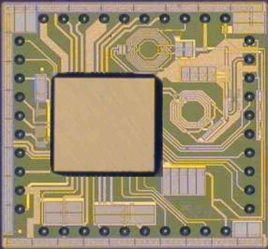
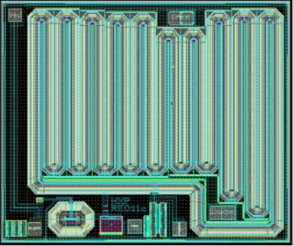
A PICS carrier seen from the top, with an active RF transceiver die flip-chipped on top of it.
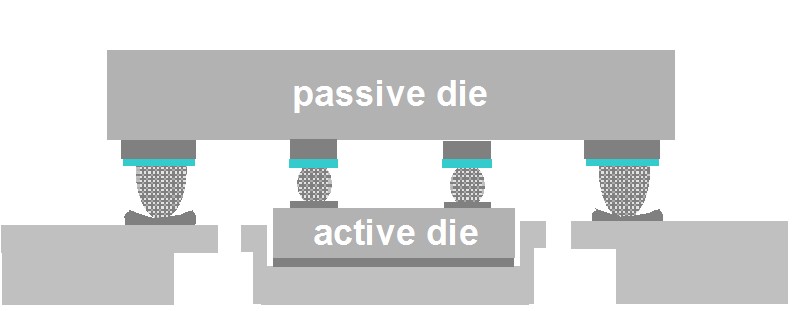
Schematic cross-section of the PICS-active assembly
|